Lab 2: Getting Started with XILINX Vivado
Create, Analyze and
Synthesis of a Full Adder Design Using XILINX Vivado WebPACK
Revised
by: Akshay Bharadwaj
Xilinx Vivado
Version: 2015.4 WebPACK Edition
Last Modified: 03-26-2016
Introduction
Xilinx Vivado is a complete FPGA logic-synthesis and optimization tool. With Xilinx Vivado, you can create optimized FPGA netlists from VHDL code. This lab will help you to learn how to create a design synthesize and implement it using Xilinx Vivado. Xilinx Vivado is available for use on both Windows and Linux based machines.
Note: -Xilinx Vivado WebPACK and Xilinx Vivado Design Suite mainly differ in the availability of IP blocks. Hence the steps shown below, though based on Xilinx Vivado WebPACK, would also work for Xilinx Vivado Design Suite edition.
Purpose
of Lab2
The purpose of this lab is to introduce students to Xilinx Vivado software. In Lab 1 you were introduced to synthesizing a simple VHDL program using Active-HDL. In this lab you will not only synthesize the VHDL code but also add constraints to the same, but in Xilinx Vivado.
Contents
· Create a Project
· Synthesize design
· Create the design implementation
· Enter Design Constraints and Controls
· Optimize a Design Implementation
Create a Project
Start Viviado 2015.4 application from the Start menu. (Start -> All Apps -> Xilinx Design Tools -> Vivado 2015.4).
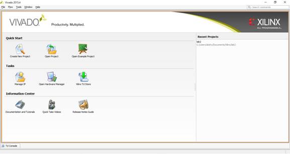
Create a new project by clicking File menu > New Project, or “Create New Project” icon from the Quick Start.
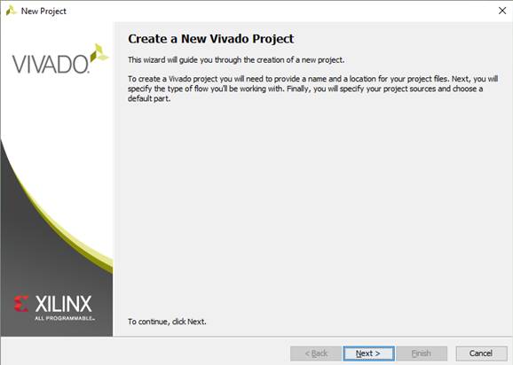
When the Create New Project window is displayed, click Next.
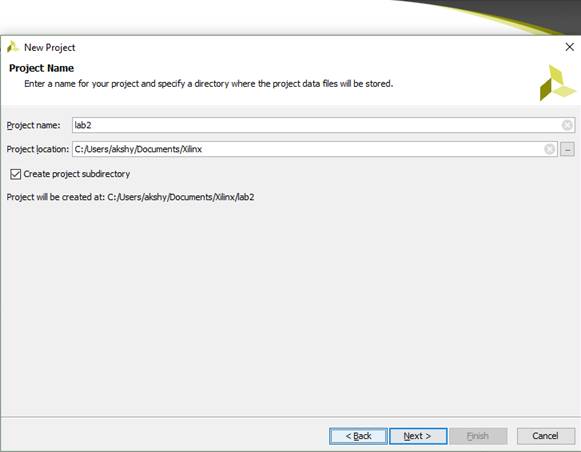
Now, choose your
working directory (or the directory where you have your Lab 1 stored) and type your new project name lab
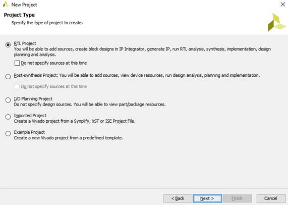
On the Project Type window,
select RTL Project and click Next.
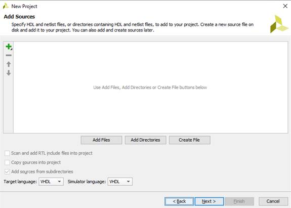
The next window allows you to add sources into the project. Make sure that the target language and simulator language selected in the bottom of the window is VHDL and click Next.
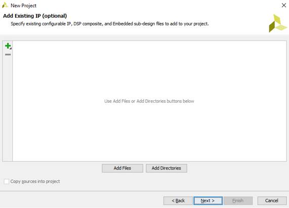
The next window allows you to add existing IP files, (since we do not need it now) click Next.
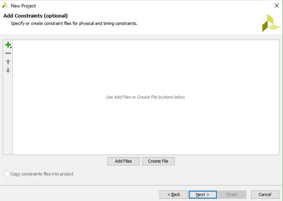
In the Add Constraints window, click Next (we shall create one later) and go to the device selection window.
In the device selection window, use the following settings to select the device.
Use the following settings to specify device and project properties.
1. Select: - Parts (default option)
2. Product Category: - General Purpose
3. Family: - Artix-7
4. Package: - cpg236
5. Speed grade: - -1
6. Temp grade: - C
Select the part “xc7a35tcpg236-1”. The Xilinx FPGA part number is XC7A35T-1CPG236C.
You could also search for “XC7A35T” in the part search bar.
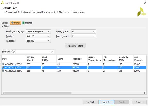
Note: - Options 2 – 6 may change if you are using a development board with a different FPGA. The options provided above are specifically for the BASYS3 board from Digilent, it uses the FPGA with part number XC7A35T-1CPG236C.
If you are using an evaluation development board from Xilinx, then select the appropriate settings for the device in the boards tab (option 1).
Note: - For the purpose of this course you can use the default settings for the remaining properties.
Note: -The various properties mainly deal with the device selection and tool settings. Try to learn about the various options available under each property.
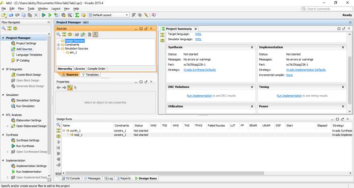
Click “Next” button and this will lead you to the “Project Summary” page of the “New Project Wizard”.
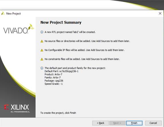
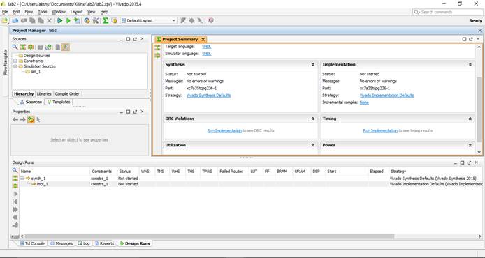
Click “Finish” to complete new project setup and go to the Project Manager window.
Create New Source You have three options in creating a new
source file.
Option 1: Use the Flow navigator toolbar on the left-hand side of the project
manager window to create a new source. Click on the add sources icon to add or create a new source.
Option 2: Use the project manager, right click on the Design Sources and select add
sources.
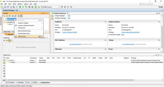
Option 3: Use the Keyboard Shortcut Alt+A.
This
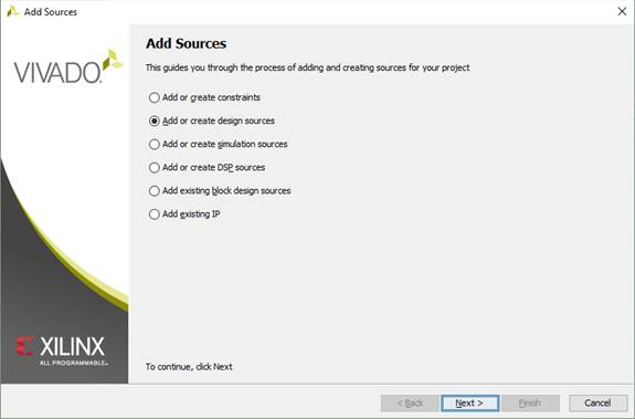
brings up the “Add Sources Wizard” with options for various source types.
Select add or create design sources
and click Next.
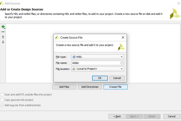
In the add or
create design sources window, click Create
File and choose VHDL from ‘File Type’ and
enter a name, “Adder”, for the new source file in the File Name field
and click OK and then click Finish.
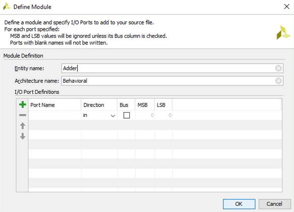
A Define Module
window will open and you will be asked to input the ports information, you can
use the wizard or you just click Cancel.
Note: -This information will be used by the tool, Xilinx Vivado,
to create a skeleton code to help you. You can edit the VHDL code generated if
needed, for eg. you can
delete, add or modify port signals that might have specified.
You will return to Xilinx Vivado
project manager and see that the new source file, Adder.vhd, has been added to
the project.
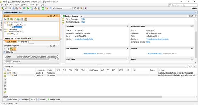
Open the Adder.vhd file by double clicking it, you can see in the
right-hand window that a template of the VHDL source file, based on information
you provided while creating the new source, is already generated for you by
Xilinx Vivado or there is an empty file ready for
editing. You need to complete the source code based on your own design
project. Here, copy and paste the following code into the Adder.vhd
file.
Note:
You should clearly understand what statements are automatically generated and
what are needed to be coded by yourself. Please compare the automatically
generated code with the following code to see this.
library ieee;
use ieee.std_logic_arith.all;
use ieee.std_logic_unsigned.all;
use
ieee.std_logic_1164.all;
entity adder is
port ( a_in : in std_logic_vector
(3 downto 0);
b_in
: in std_logic_vector (3 downto 0);
c_out
: out std_logic_vector (3 downto
0));
end adder;
architecture adder_arch of adder is
begin
process (a_in, b_in)
variable carry : std_logic_vector
(4 downto 0);
variable sum :std_logic_vector
(3 downto 0);
begin
carry (0) := '0';
for i in 0 to 3 loop
sum (i)
:= a_in(i) xor b_in(i)
xor carry(i);
carry (i+1) := (a_in(i) and b_in(i)) or
(b_in(i) and carry (i)) or
(carry (i) and a_in(i));
end loop;
c_out <= sum;
end process;
end adder_arch;
Synthesize design
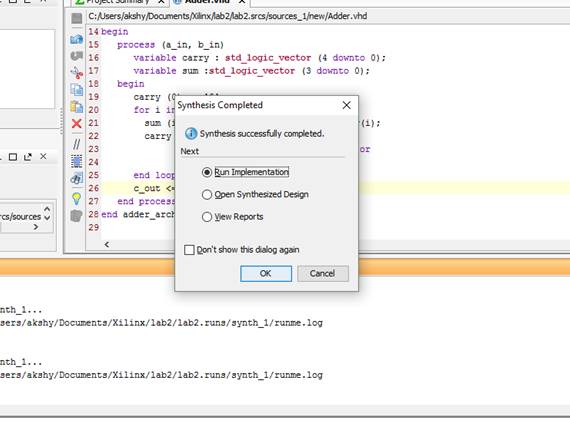
o Save the file by click Save under file menu or using the keyboard shortcut Ctrl + S.
o Click Run Synthesize in "Flow Navigator" window to start the synthesizing process, or use the keyboard shortcut F11 to run synthesis, or click on the Run Synthesis button from the toolbar.
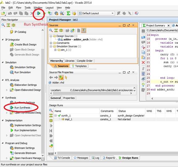
o When this process is finished, “Synthesize Completed" pop up appears on the screen, click Cancel. If you click OK, it will run implementation (We don’t want to do that at this point of time).
Note:
o Synthesis is the process of converting the abstract circuit behavior, described by a VHDL (or any HDL) code, into a hardware implementation in terms of logic gates.
o To observe the results of the synthesis, expand Synthesize in "Flow Navigator" window (click on the + sign). The "Flow Navigator" window with Synthesize expanded is shown below.
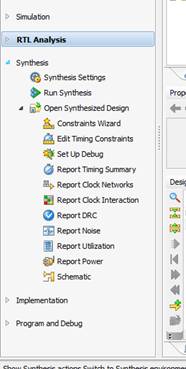
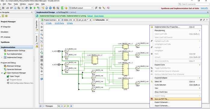
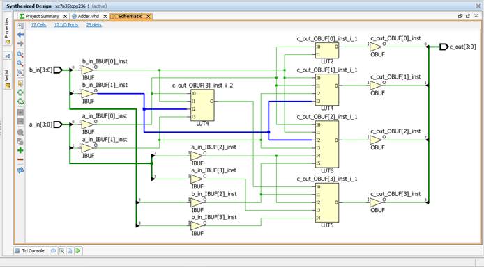
o To view the register transfer level (RTL) schematic, click on “Schematic”
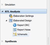
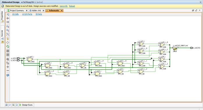
o To view the Netlist or gate level schematic, expand “RTL Analysis” and expand “Elaborated Design”. Click on “Schematic”.
Create the design implementation
o First we need to assign the pin usage for the chip.
o Add user constraints file to the project. The process is similar to that of adding the “adder.vhd” source file earlier. For example, in the “Project Manager”, right-click and select “Add Sources”.
o Choose Add or create constrains and enter a name for the new source file, pin_io, in the File Name field and click OK.
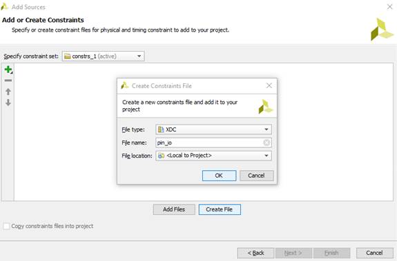
o Next click Finish.
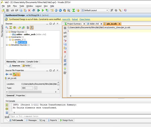
o
In the Hierarchy
section of Project Manager, expand
constraints (and any other subfolder) to find the added constraints file.
Double click file to open it in the editor to edit the file.
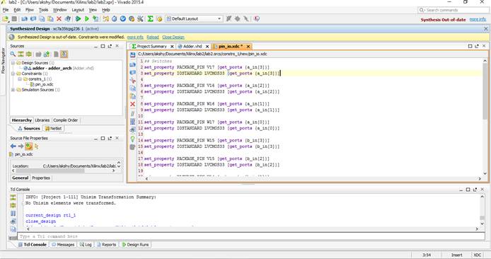
o Entering Design Constraints by copying and
pasting the following into your user constraint file (pin_io.xdc). This is the
pin assignment for our Artix 7 device. You’d better understand the syntax of the constrains files and you will be required to assign the
pins by yourself in your final projects.
Note: -The user constraints file (or implementation constraints file) is used
to specify the actual pins on the FPGA to which the ports in the top most
entity are mapped. Except for some specific pins, JTAG, power or clock, most
pins on an FPGA are I/O. That is, the pins can either be used as an input or
output based on the program. In practice, FPGAs in all applications would have
been mounted on a board with peripheral devices and thus specifying pins as
either inputs or outputs based on peripheral connections. If a design is
implemented without the constraints file the tool will, if it does not give an
error (due to absence of the constraints file), map the ports according to some
internal criteria (shortest delay or smallest area) and the pins so used might
not be appropriate based on the peripheral devices mounted on the board with the
FPGA.
# Pin assignment for SWs / Inputs
set_property PACKAGE_PIN V17 [get_ports {a_in[3]}]
set_property IOSTANDARD LVCMOS33 [get_ports {a_in[3]}]
set_property PACKAGE_PIN V16 [get_ports {a_in[2]}]
set_property IOSTANDARD LVCMOS33 [get_ports {a_in[2]}]
set_property PACKAGE_PIN W16 [get_ports {a_in[1]}]
set_property IOSTANDARD LVCMOS33 [get_ports {a_in[1]}]
set_property PACKAGE_PIN W17 [get_ports {a_in[0]}]
set_property IOSTANDARD LVCMOS33 [get_ports {a_in[0]}]
set_property PACKAGE_PIN W15 [get_ports {b_in[3]}]
set_property IOSTANDARD LVCMOS33 [get_ports {b_in[3]}]
set_property PACKAGE_PIN V15 [get_ports {b_in[2]}]
set_property IOSTANDARD LVCMOS33 [get_ports {b_in[2]}]
set_property PACKAGE_PIN W14 [get_ports {b_in[1]}]
set_property IOSTANDARD LVCMOS33 [get_ports {b_in[1]}]
set_property PACKAGE_PIN W13 [get_ports {b_in[0]}]
set_property IOSTANDARD LVCMOS33 [get_ports {b_in[0]}]
# Pin assignment for LEDs / Output
set_property PACKAGE_PIN U16 [get_ports {c_out[0]}]
set_property IOSTANDARD LVCMOS33 [get_ports {c_out[0]}]
set_property PACKAGE_PIN E19 [get_ports {c_out[1]}]
set_property IOSTANDARD LVCMOS33 [get_ports {c_out[1]}]
set_property PACKAGE_PIN U19 [get_ports {c_out[2]}]
set_property IOSTANDARD LVCMOS33 [get_ports {c_out[2]}]
set_property PACKAGE_PIN V19 [get_ports {c_out[3]}]
set_property IOSTANDARD LVCMOS33 [get_ports {c_out[3]}]
Note: The lines in the .xdc file are read as follows:
1. “#” indicates the beginning of comments. Note: Comment in VHDL file (.vhd file) start with “--" (two hypens) while comments in constraints file (.xcd file) start with “#” (hash).
2. Line 2 of pin_io.xcd, shown above, is: set_property PACKAGE_PIN V17 [get_ports {a_in[3]}]
and is read as follows:
a) set_property is the predefined word to set or initialize a property or a feature in the design.
b) PACKAGE_PIN V17 specifies a specific placement of a top-level port in the logical design to a physical package pin on the device and “V17” being the pin no on the FPGA.
Note: On the Digilent board you can read the names of the I/O pins that the buttons (btn), switches, LEDs or seven segment displays are connected.
c) get_ports {a_in[3]} refers to the MSB (Most Significant Bit) of port a_in, i.e. a_in[3], in the VHDL code provided at the begining.
3.
Line 3 of pin_io.xcd, set_property IOSTANDARD LVCMOS33 [get_ports {a_in[3]}]
sets the IO standard of the port to LVCMOS 3.3 Volts.
Note: If you
don’t want to specify the IO standard for the ports use the following command
in the .xdc file. set_property SEVERITY {Warning} [get_drc_checks
NSTD-1]
o
Use the
online help if you need instructions and information about specific
constraints, attributes, and optimization options.
o
If
later you find default constraints are not sufficient for your requirements,
you might have to repeat creating and optimizing implementations to enter
constraints.
o
Save
the constraints file.
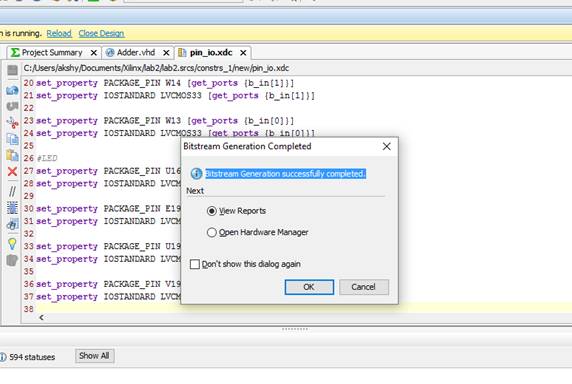
Generate Programming File
o Under the Flow Navigator window, select Program and Debug and click on Generate Bitstream, or you can click on the icon for Generate Bitstream in the toolbar as highlighted below.
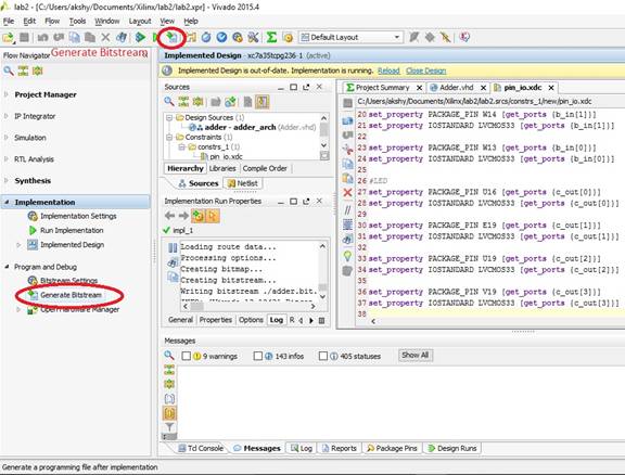
o If the “Generate Bitstream”
process is successfully completed, a pop-up message “Bitstream Generation successfully completed” is displayed in the console window.
o
The
design summary tab lists the summary of the design, including any errors or
warnings. This can be accessed from Project -> Design Summary/Reports in the
dropdown menu.
o
In
later labs we will produce workable bit file for more advanced circuits that
can also be download to the board. The basic procedures are as this lab.
o
The
whole process is well logged and the intermediate files can be used in other
XILINX tools.
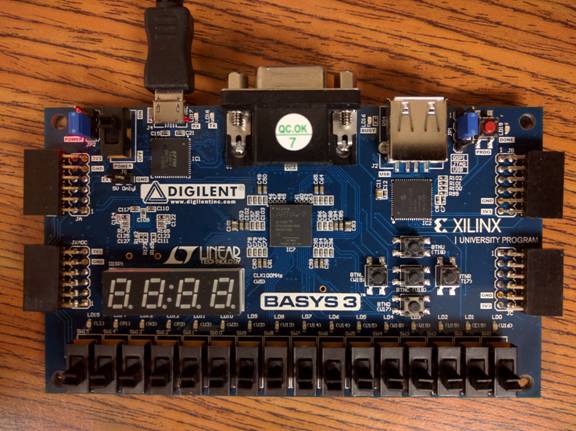
Program the FPGA on Basys3 Development Board
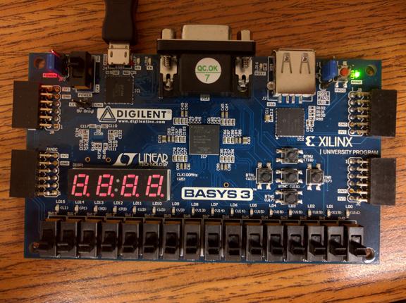
o Connect the board to your computer using the USB cable provided and make sure that jumper JP1 is configured to JTAG.

o Click here to find the reference manual for Basys 3 reference board.
o From the “Flow Navigator” expand Program and Debug and select “Open Hardware Manager”. Under Open Hardware Manager click Open Target and click “Auto Connect”, or click the Auto Connect icon In the toolbar indicated below.
![]()
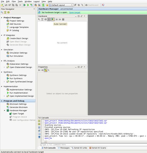
o If the development board is connected and turned on, Hardware manager should detect the board (Xilinx_tcf/Digilent/…) and device on the same (FPGA: xc7a35t_0).
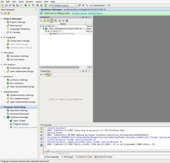
o Right click on the device and select “Program Device” or select “Program Device” from the Flow Navigation Window.
o On the file Open window that pops up, navigate to the directory containing the lab2 project folder and select the .bit file (the software usually has the correct .bit file by default) in this case “adder.bit”.
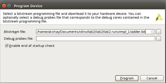
o Click “Program” to program the FPGA. If the programming is successful, LED LD19 will turn green.

o The FPGA has now been successfully programmed.
Note: -Do not disconnect or turn off the board yet.
o With the board having been programmed you can now verify your design. Remember, from the User/Implementation constraints file, that the first eight of the sixteen switches are used as inputs (four for “a_in” and four for “b_in) and first four LED’s are used for “c_out”. Provide various input combinations using the switches and verify that the outputs are correct. Note: -The entity does not have “carry in” or “carry out”.
o
After
verifying the design, you can switch off the power supply to the development
board and disconnect it from your computer.
Requirement
- Write a lab report. (Limit to Max of 3 Pages.)
- Solutions to the following Questions. (Limit to Max of 2 Pages)
- What can you infer from, the Outputs in the Console window and the Design Summary tab?
- What are the factors that come into picture in selecting a FPGA for your design implementation?
Submit your lab report and solutions to questions before lab 3.
Note:
1. For the lab report you can use the template: Lab report template. The link is also available near the end of the lab index page.
2. The VHDL files are available in the project working directory. For example the above project (lab2) was created in “D:\VHDL_Designs\” and hence its working directory would be “D:\VHDL_Designs\lab2” and all the VHDL source files are available in that directory.
3. To include the RTL, schematics in your report, right click on the schematic and select “Save as PDF”. Save the PDF in the desired location on the system.