Lab 2: Getting Started with XILINX Vivado
Create, Analyze and Synthesize
of a Full Adder Design Using XILINX Vivado WebPACK
Xilinx Vivado
Version: 2015.4 WebPACK Edition
Last Modified: 03-26-2016
Introduction
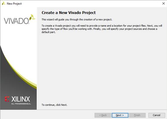
Xilinx Vivado is a complete FPGA logic-synthesis and optimization tool. With Xilinx Vivado, you can create optimized FPGA netlists from VHDL code. This lab will help you to learn how to create a design synthesize and implement it using Xilinx Vivado. Xilinx Vivado is available for use on both Windows and Linux based machines.
Note: -Xilinx Vivado WebPACK and Xilinx Vivado Design Suite mainly differ in the availability of IP blocks. Hence the steps shown below, though based on Xilinx Vivado WebPACK, would also work for Xilinx Vivado Design Suite edition.
Purpose
of Lab2
The purpose of this lab is to introduce students to Xilinx Vivado software. In Lab 1 you were introduced to synthesizing a simple VHDL program using Active-HDL. In this lab you will not only synthesize the VHDL code but also add constraints to the same, but in Xilinx Vivado.
You may use or modify the following code to implement a full adder.
library
ieee;
use ieee.std_logic_arith.all;
use ieee.std_logic_unsigned.all;
use
ieee.std_logic_1164.all;
entity adder is
port ( a_in : in std_logic_vector
(3 downto 0);
b_in
: in std_logic_vector (3 downto 0);
c_out
: out std_logic_vector (3 downto
0));
end adder;
architecture adder_arch of adder is
begin
process (a_in, b_in)
variable carry : std_logic_vector
(4 downto 0);
variable sum :std_logic_vector
(3 downto 0);
begin
carry (0) := '0';
for i in 0 to 3 loop
sum (i)
:= a_in(i) xor b_in(i)
xor carry(i);
carry (i+1) := (a_in(i) and b_in(i)) or
(b_in(i) and carry (i)) or
(carry (i) and a_in(i));
end loop;
c_out <= sum;
end process;
end adder_arch;
You
must complete the following steps using Vivado tool
o
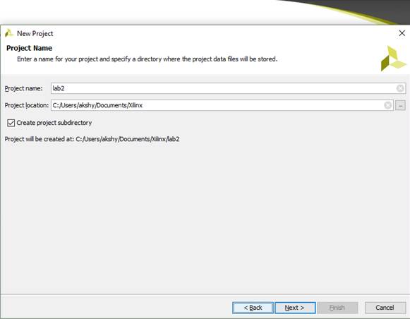
Create a Project
o
Create New Source
o
Synthesize design
o
Create the design implementation
o
Enter Design Constraints and Controls
o Generate
Programming File
o
Program the FPGA on Basys3 Development Board
o To implement the last step connect the board to your computer using the USB cable provided and make sure that jumper JP1 is configured to JTAG.

o Click here to find the reference manual for Basys 3 reference board.
o From the “Flow Navigator” expand Program and Debug and select “Open Hardware Manager”. Under Open Hardware Manager click Open Target and click “Auto Connect”.
o If the development board is connected and turned on, Hardware manager should detect the board (Xilinx_tcf/Digilent/…) and device on the same (FPGA: xc7a35t_0).
o Right click on the device and select “Program Device” or select “Program Device” from the Flow Navigation Window.
o On the file Open window that pops up, navigate to the directory containing the lab2 project folder and select the .bit file (the software usually has the correct .bit file by default) .
o Click “Program” to program the FPGA. If the programming is successful, LED LD19 will turn green.

o
With the board having been programmed you can
now verify your design. Provide various input combinations using the switches
and verify that the outputs are correct.
o
After
verifying the design, you can switch off the power supply to the development
board and disconnect it from your computer.
Requirement
- Write a lab report. (Limit to Max of 3 Pages.)
- Solutions to the following Questions. (Limit to Max of 2 Pages)
- What can you infer from, the Outputs in the Console window and the Design Summary tab?
- What are the factors that come into picture in selecting a FPGA for your design implementation?
Submit your lab report and solutions to questions before lab 3.
Note:
1. For the lab report you can use the template: Lab report template. The link is also available near the end of the lab index page.
2. To include the RTL, schematics in your report, right click on the schematic and select “Save as PDF”. Save the PDF in the desired location on the system.