Lab 4:
Revised
by: Akshay Bharadwaj
Xilinx Vivado Version: 2015.4 WebPACK
Last modified: 03-29-2016
Introduction
In this lab,
you will create a 4-bit adder with carry input and output along with a clock
enable by using the Xilinx CORE Generator and instantiate the Adder
Objectives
After completing this lab, you will be able to:
· Generate a CORE Generator macro
· Synthesize the VHDL and black-box instantiations through synthesis
· Implement a synthesized design through the Xilinx implementation tools
Design Description
Use the CORE Generator to create
a 4-bit adder that has the following characteristics:
· Two input data width of 4-bits of unsigned data
· Carry in and out.
· Clock enable
· Asynchronous output data width of 4 bits.
Procedure
Start the Project Navigator and Open the Project
Step 1: Start the Xilinx Vivado from the Start menu
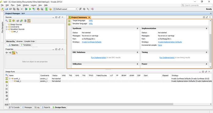
Step 2: Create a new project called lab4. Refer to lab2 in case you need help with creating the project.
At the end of Step 2, you should have an empty project with the correct device and project settings setting.
Generate a 4-bit Adder
Using the CORE Generator
In this procedure, you learn how to generate and add a IP CORE Generator ADDER to your Vivado project.
To create and add the Adder-Subtracter macro, perform the following steps:
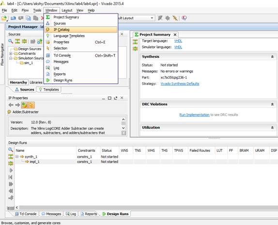
Step 1:
Go to Window
and select IP catalog. OR you
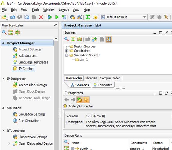
can also select IP catalog from Flow Navigator window under Project Manager.
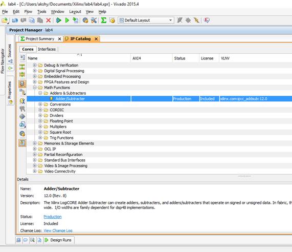
Step 2:
IP Catalog opens up on the right side on the
edit window. Among the IP Cores, scroll down to Math Functions and expand (+
marker). You should be able to find several math functions, but we are
interested in Adders & Subtarcters, hence
expand it. You should find the Adder/Subtracter IP Core. Double click the IP
core.
Step 3: This brings up the “Customize IP” window.
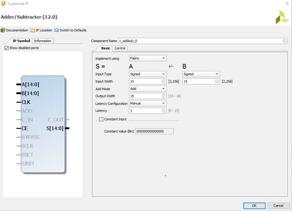
Step 4: Customize the IP core with the specifications previously mentioned. You can rename the component if you prefer to in the Component Name field. After you finish customization, click OK.
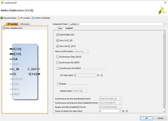
Note: You need to use both Basic and Control tabs to customize the IP according to the needed specifications.

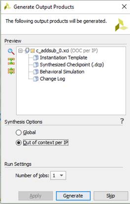
Step 5: A Generate Output Products will popup. Click Generate.
Note: Look at the files in the window, when you generate the IP those files will be generated. Instantiation Template file is required in the later step.
Note: If you are interested, you can
read the datasheet by clicking
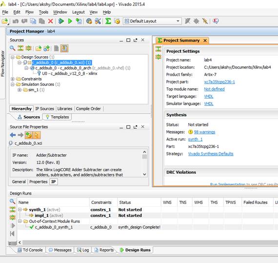
Step 6: Your IP Core should be generated and added to the project.
.
Adding the CORE Generator Macro intoYour VHDL Code
The
c_addsub_0 (the component name if you renamed) macro will need to be declared
and instantiated (black-boxed) into a top-level VHDL file.
To
instantiate the Adder-Subtracter, perform the following steps:
Step 1:
Create a new Top Module file name adder_top.vhd (Refer to instruction in
lab2 if you have difficulties creating a file) with the following ports
·
4-bit
input (Operand A)
·
4-bit
input (Operand B)
·
Clock
(Input Clock)
·
Clock
Enable (Control Input)
·
Carry
In (Input)
·
Carry
Out (Output)
·
4-bit
Output (Result)
Check
with the Sample code below.
library IEEE;
use IEEE.STD_LOGIC_1164.ALL;
use IEEE.STD_LOGIC_UNSIGNED.ALL;
entity adder_top is
Port ( a_in : in
STD_LOGIC_VECTOR (3 downto 0);
b_in : in
STD_LOGIC_VECTOR (3 downto 0);
clk : in
STD_LOGIC;
clk_en : in
STD_LOGIC;
carry_in : in
STD_LOGIC;
carry_out : out STD_LOGIC;
c_out : out
STD_LOGIC_VECTOR (3 downto 0));
end adder_top;
architecture Behavioral of adder_top is
begin
end Behavioral;
Step 2:
In the Project Manager window, go to IP Sources tab, select the IP core
generated and expand the Instantiation
Template subfolder. Open the .vho file (here c_addsub_0.vho).
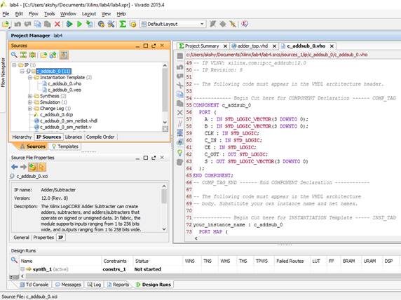
Step 3:
Copy the Component declaration from the template
(.vho file) and go back to top module file adder_top.vhd
previously created and paste it right after the declaration of architecture and
before begin. Your architecture should look something like this
architecture
Behavioral of adder_top is
COMPONENT
c_addsub_0
PORT (
A : IN STD_LOGIC_VECTOR(3 DOWNTO 0);
B : IN STD_LOGIC_VECTOR(3 DOWNTO 0);
CLK : IN STD_LOGIC;
C_IN : IN STD_LOGIC;
CE : IN STD_LOGIC;
C_OUT : OUT STD_LOGIC;
S : OUT STD_LOGIC_VECTOR(3 DOWNTO 0)
);
END
COMPONENT;
begin
end
Behavioral;
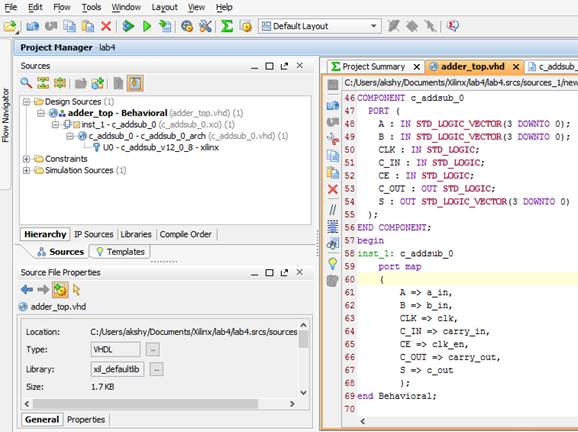
Step 4:
Finally, the component has to be port mapped you can
use the following code for the portmap.
inst_1:
c_addsub_0
port map
(
A => a_in,
B => b_in,
CLK => clk,
C_IN => carry_in,
CE => clk_en,
C_OUT => carry_out,
S => c_out
);
Step 5:
Save the file. After instantiation, in the
Hierarchy window, adder_top.vhd
should be recognized as the top module. In case it is not recognized as top
module there could be an error in the instantiation, please check your
instantiation again.
Note: For your reference,
your code should be similar to
library IEEE;
use
IEEE.STD_LOGIC_1164.ALL;
use
IEEE.STD_LOGIC_UNSIGNED.ALL;
entity adder_top is
Port ( a_in : in STD_LOGIC_VECTOR (3 downto
0);
b_in : in STD_LOGIC_VECTOR (3 downto
0);
clk : in STD_LOGIC;
clk_en : in STD_LOGIC;
carry_in : in STD_LOGIC;
carry_out : out STD_LOGIC;
c_out : out STD_LOGIC_VECTOR (3
downto 0));
end adder_top;
architecture
Behavioral of adder_top is
COMPONENT
c_addsub_0
PORT (
A : IN STD_LOGIC_VECTOR(3 DOWNTO 0);
B : IN STD_LOGIC_VECTOR(3 DOWNTO 0);
CLK : IN STD_LOGIC;
C_IN : IN STD_LOGIC;
CE : IN STD_LOGIC;
C_OUT : OUT STD_LOGIC;
S : OUT STD_LOGIC_VECTOR(3 DOWNTO 0)
);
END COMPONENT;
begin
inst_1: c_addsub_0
port map
(
A => a_in,
B => b_in,
CLK => clk,
C_IN => carry_in,
CE => clk_en,
C_OUT => carry_out,
S => c_out
);
end Behavioral;
Synthesize the whole design.
Please refer to lab2.
Conclusion
You learned the basic design flow for taking a VHDL design with IP CORE Generator macros through the design process, which includes the following:
· Understanding the basics for generating a IP CORE Generator macro
· Knowing how to synthesize a design containing IP CORE Generator macros through synthesis.
Try It Out:
Implement this design on to your board. Create the necessary Constraints File. Please refer to lab2 for additional details.
You can use the following for the constraint file
##
Switches
set_property
PACKAGE_PIN V17 [get_ports {a_in[0]}]
set_property
IOSTANDARD LVCMOS33 [get_ports {a_in[0]}]
set_property
PACKAGE_PIN V16 [get_ports {a_in[1]}]
set_property
IOSTANDARD LVCMOS33 [get_ports {a_in[1]}]
set_property
PACKAGE_PIN W16 [get_ports {a_in[2]}]
set_property
IOSTANDARD LVCMOS33 [get_ports {a_in[2]}]
set_property
PACKAGE_PIN W17 [get_ports {a_in[3]}]
set_property
IOSTANDARD LVCMOS33 [get_ports {a_in[3]}]
#########################################################################
set_property
PACKAGE_PIN W2 [get_ports {b_in[0]}]
set_property
IOSTANDARD LVCMOS33 [get_ports {b_in[0]}]
set_property
PACKAGE_PIN U1 [get_ports {b_in[1]}]
set_property
IOSTANDARD LVCMOS33 [get_ports {b_in[1]}]
set_property
PACKAGE_PIN T1 [get_ports {b_in[2]}]
set_property
IOSTANDARD LVCMOS33 [get_ports {b_in[2]}]
set_property
PACKAGE_PIN R2 [get_ports {b_in[3]}]
set_property
IOSTANDARD LVCMOS33 [get_ports {b_in[3]}]
#########################################################################
set_property
PACKAGE_PIN W5 [get_ports {clk}]
set_property
IOSTANDARD LVCMOS33 [get_ports {clk}]
#########################################################################
set_property
PACKAGE_PIN W14 [get_ports {clk_en}]
set_property
IOSTANDARD LVCMOS33 [get_ports {clk_en}]
set_property
PACKAGE_PIN V15 [get_ports {carry_in}]
set_property
IOSTANDARD LVCMOS33 [get_ports {carry_in}]
#########################################################################
set_property
PACKAGE_PIN U16 [get_ports {c_out[0]}]
set_property
IOSTANDARD LVCMOS33 [get_ports {c_out[0]}]
set_property
PACKAGE_PIN E19 [get_ports {c_out[1]}]
set_property
IOSTANDARD LVCMOS33 [get_ports {c_out[1]}]
set_property
PACKAGE_PIN U19 [get_ports {c_out[2]}]
set_property
IOSTANDARD LVCMOS33 [get_ports {c_out[2]}]
set_property
PACKAGE_PIN V19 [get_ports {c_out[3]}]
set_property
IOSTANDARD LVCMOS33 [get_ports {c_out[3]}]
set_property
PACKAGE_PIN L1 [get_ports {carry_out}]
set_property
IOSTANDARD LVCMOS33 [get_ports {carry_out}]